|
Plasma
etch, RTP, and CVD deposition processes rely
on the stiffness, high thermal conductivity,
and chemical resistance of CVD SiC components.
Conductive silicon carbide components open up
new ways to get energy into the chamber. Crucibles
of PBN, a unique material with anisotropic properties,
provide outstanding performance in gallium arsenide
(GaAs) crystal production and molecular beam
epitaxy (MBE).
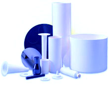
Our
advanced ceramics Performance PBN and Performance
SiC have an impressive list of attributes:
chemically inert; theoretically dense; highly
machinable; low outgasing at elevated temperatures;
high resistance to oxidation at elevated temperatures;
retention of thermal and mechanical properties
at temperatures beyond 2000° C; product
deposition to "near net" shapes; availability
in many shapes and sizes, including large flat
plates; the intrinsic purity typical of the
chemical vapor deposition process.
Flokal works
with your chemical, physical, electrical, and
mechanical requirements to create innovative
advanced ceramic solutions quickly, and with
the quality you expect, to satisfy your most
demanding applications. There are many benefits
to using our materials in your manufacturing
processes: improve your production processes
and product quality; drop particle counts as
much as 50% in applications where PerformanceSiC
silicon carbide replaces other materials; shorten
new product times to market; reduce the costs
of ownership of your equipment; increase life
of consumables.
Our
materials provide superior performance in many
applications in both semiconductor and compound
semiconductor processing.
Semiconductor
Dry Etch RTP CVD: susceptors; processing
chambers; liners; gas distribution plates; wafer
carriers; edge rings; electrostatic chucks;
sputter targets; heating elements; electrodes;
RF components.
Compound
Semiconductor and Microwave GaAs crystal
growth MBE: crucibles; heating elements;
auxiliary effusion cell hardware.
|